This post describes two examples of control software configurations for multicore MCU.
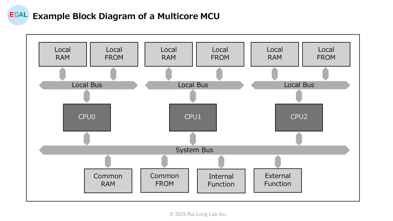
Example Block Diagram of a Multicore MCU
The block diagram of a multicore MCU will introduce the control software configuration using an SMP (Symmetric Multi-Processing) block diagram as an example, as shown below.
Example of software function placement by CPU
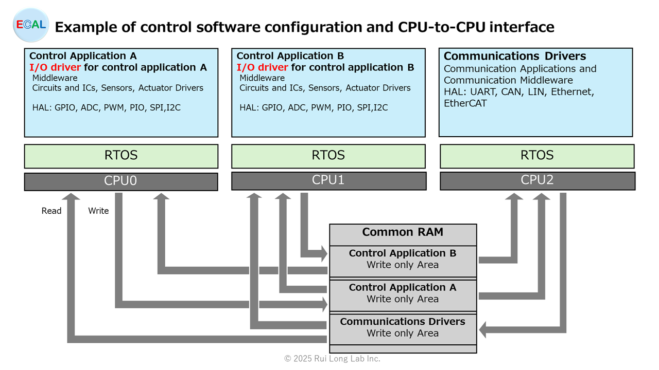
Example of control software configuration and CPU-to-CPU interface
Example of control software configuration
The control software configuration divides functions among CPUs as shown in the diagram and table below. Note that this assumes sufficient processing time for each CPU.
| CPU | Software |
|---|---|
| CPU0 | Control Application A Control Application B Control Application C |
| CPU1 | I/O Drivers – Operation and I/O drivers for circuits, ICs, sensors, actuators, etc. – HAL:GPIO, ADC, PWM, Pulse IO, SPI, I2C |
| CPU2 | Communications Drivers – Communication Applications and Communication Middleware – HAL:UART, CAN, LIN, Ethernet, EtherCAT |
Example of CPU-to-CPU interface
The CPU-to-CPU interface is implemented via the Common RAM, as shown in the diagram below. Each CPU has a dedicated Write-only Area, into which data is written only once per processing cycle. This write operation employs mutual exclusion control to ensure data integrity. Other CPUs read the necessary information from this Write-only Area.
| Write | Read |
|---|---|
| CPU0: Control application A/B/C | CPU1: I/O Drivers CPU2: Communications Drivers |
| CPU1: I/O Drivers | CPU0: Control application A/B/C |
| CPU2: Communications Drivers | CPU0: Control application A/B/C |

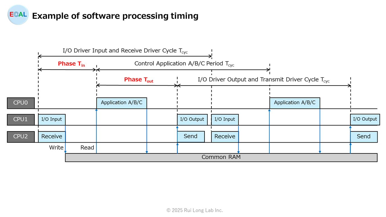
Example of software processing timing
The software processing timing is as shown in the figure below.
| Label | Times |
|---|---|
| Tcyc | CPU0: Processing cycle of control application A/B/C CPU1: I/O driver processing cycle CPU2: Communication driver processing cycle |
| Tin | Phase from CPU1 I/O driver input and CPU2 communication driver reception processing start to CPU0 control application processing start. Note: Tin indicates the maximum time required for I/O input and reception processing, plus a margin. These processes must be completed before the control application begins execution. |
| Tout | Phase from the start of CPU0 control application processing to the start of CPU1 I/O driver output and CPU2 communication driver transmission processing. Note: Tout indicates the value obtained by adding a margin of time to the maximum processing time of the control application. I/O output and transmission processing must be executed after the control application has completed. |
Example of CPU-Specific Control Application and I/O Driver Placement
Example of control software configuration and CPU-to-CPU interface
Example of control software configuration
The control software configuration divides control applications and I/O drivers per CPU as shown in the diagram and table below. Note that this assumes sufficient processing time for each CPU.
| CPU | Software |
|---|---|
| CPU0 | Control Application A I/O Drivers for Control Application A – Operation and I/O drivers for circuits, ICs, sensors, actuators, etc. – HAL:GPIO, ADC, PWM, Pulse IO, SPI, I2C |
| CPU1 | Control Application B I/O Drivers for Control Application B – Operation and I/O drivers for circuits, ICs, sensors, actuators, etc. – HAL:GPIO, ADC, PWM, Pulse IO, SPI, I2C |
| CPU2 | Communications Drivers – Communication Applications and Communication Middleware – HAL:UART, CAN, LIN, Ethernet, EtherCAT |
Note: Since MCU functions are shared resources, do not share the I/O driver for Control Application A with the I/O driver for Control Application B.
Example:
・I/O driver for control application A: ADC Gr0 ch0, ch1, ch2
・I/O driver for control application B: ADC Gr0 ch3, ch4
Using ADC Gr0 for both applications as shown above may cause malfunctions due to conflicts.
In this case, assign one of the I/O drivers to a different resource, such as ADC Gr1.
Example of CPU-to-CPU interface
The CPU-to-CPU interface is implemented via the Common RAM, as shown in the diagram below.
Each CPU has a dedicated Write-only Area, into which data is written only once per processing cycle. This write operation employs mutual exclusion control to ensure data integrity.
Other CPUs read the necessary information from this Write-only Area.
| Write | Read |
|---|---|
| CPU0: Control application A | CPU1: Control application B CPU2: Communications Drivers |
| CPU1: Control application B | CPU0: Control application A CPU2: Communications Drivers |
| CPU2: Communications Drivers | CPU0: Control application A CPU1: Control application B |
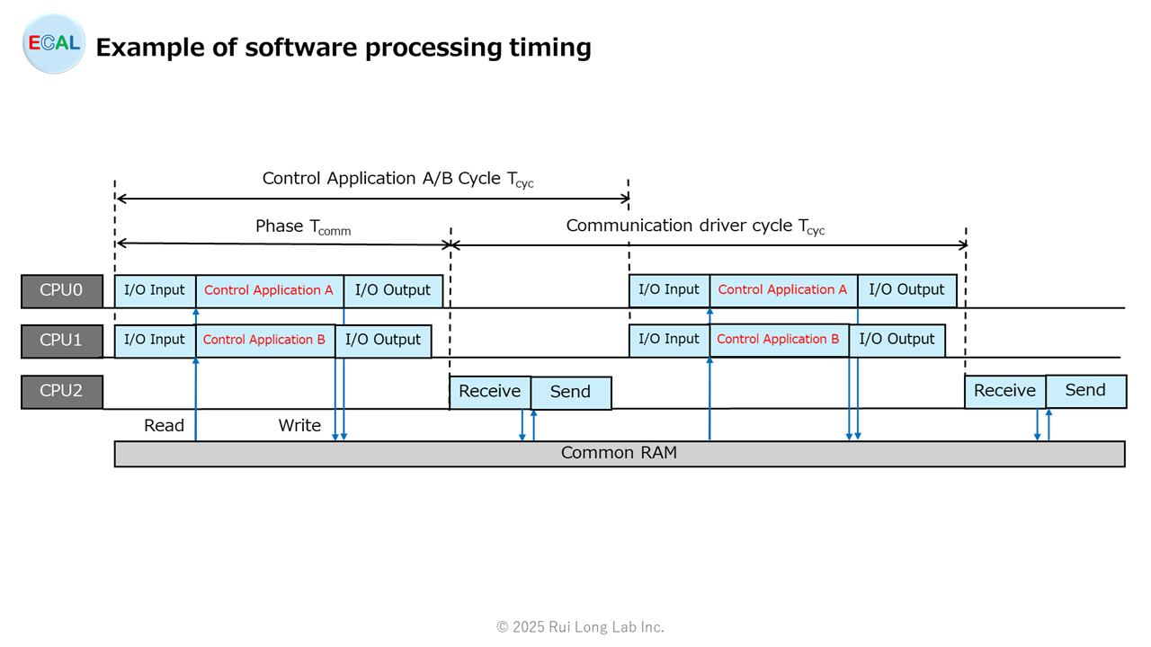
Example of software processing timing
The software processing timing is as shown in the figure below.
Note:
This example shows the processing timing when the coordination between Control Application A and Control Application B is low. If coordination is high, establish a phase in the processing timing.
| Label | Times |
|---|---|
| Tcyc | CPU0: Processing cycle of control application A CPU1: Processing cycle of control application B CPU2: Communication driver processing cycle |
| Tcomm | Phase from the start of processing control applications A/B and I/O driver inputs for CPU0 and CPU1 to the start of processing the communication driver for CPU2. |